

The rapid evolution of photovoltaic modules
The rapid evolution of photovoltaic modules
02/06/2021
In recent months we are witnessing a very rapid evolution of photovoltaic modules, in a race to improve efficiency and reduce the specific cost of photovoltaic plants (their LCOE, or Levelized Cost of Energy).
Not surprisingly, cost reductions associated with the modules expected for the next 10 years, are of the order of 17%.
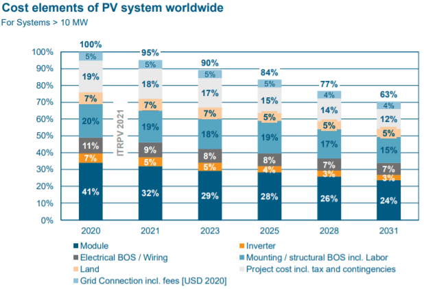
Illustration 1 – Evolution of the expected costs in plants> 10 MW, [2]
This article tries to give context to current technologies, as well as the most promising ones in the coming years. We will analyze in more detail the modules based on silicon wafers, the most common today:
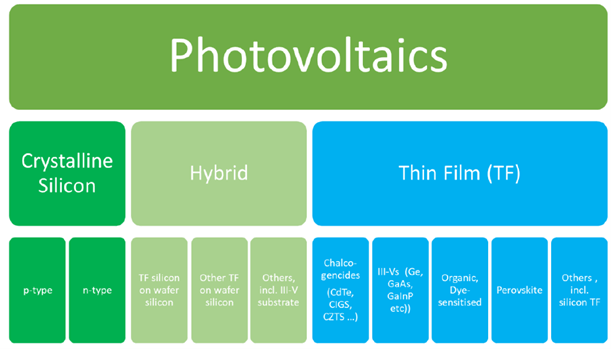
Illustration 2 – Photovoltaic technologies, [1]
Within silicon wafers, they are classified based on doping, crystallization microstructure, and cell architecture. In the following graph you can see the different sub-categories:
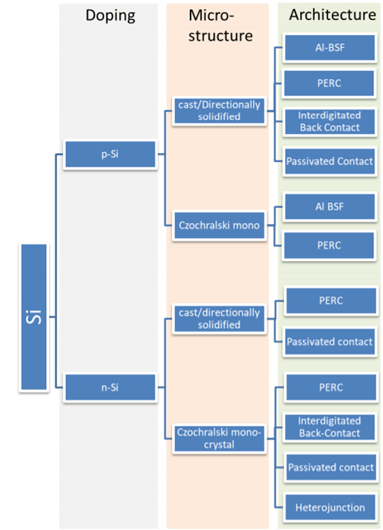
Illustration 3 – Silicon wafer sub-technologies, [1]
Considering wafer doping, the following subcategories are defined:
- P-type (the cell is built on a positively doped silicon base): It is the technology currently used in most of the modules.
- N-type (the cell is built on a Negatively doped silicon base): although the solar cells initially developed by Bell Laboratories in the 1950s used this type of doping, later development opted more for p-types, as they were more immune to radiation present in space (which was the main application of this technology in its early days).
Although we already have some commercial products with this technology, in the coming years a total shift towards it is expected, mainly derived from its greater efficiency, immunity to Oxygen-Boron defects, and being LID free.
Its current challenges for such a turn would be its higher current cost, derived mainly from the greater number of steps required in its manufacture.
Taking into account the crystallization microstructure, the following subcategories are defined:
- Polycrystalline, which accounted for more than 80% of the market until 5 years ago.
- Monocrystalline, which has totally displaced the polycrystalline (expected to be somewhat residual in the next few years).
After the growth of monocrystalline p-type technology, reaching almost 80% of the market, it can be seen that in the next few years it is expected to give way to monocrystalline n-type technologies with penetrations of 50% in the next 10 years:
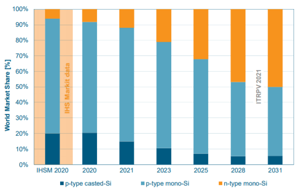
Illustration 4 – Market distribution for the different types of wafer, [2]
Finally, taking into account the architecture / cell technology, these would be the most relevant or promising technologies:
- Al-BSF (Aluminum Diffused Back Surface Field)
It has been the market standard until 2010.
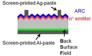
Illustration 5 – AL-BSF cell section (not to scale), [1]
- PERC (Passivated Rear Emitter Contact)
Developed in the 80s / 90s at the University of New South Wales (UNSW) in Sydney.It is being the new market standard as of 2010.

Illustration 6 – PERC cell section (not to scale), monophasic and bifacial, [1]
- N-type TOPCON (Tunnel Oxide Passivated CONtact)
Developed by the Fraunhofer Institute for Solar Energy Systems in Germany in 2013. One of the most promising technologies to succeed the p-type PERC.
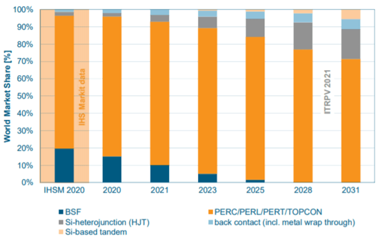
Illustration 7 – Market distribution for different cell technologies, [2]
Its main advantage, in addition to expected efficiency increases of around 1%, is that PERC manufacturing lines can be adapted for this technology, with minimal changes.
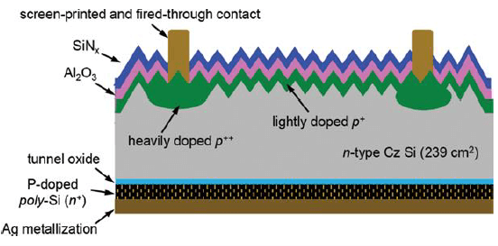
Illustration 8 – TOPCon cell section (not to scale), [1]
- N-Type HJT (Heterojunction)
Developed by Sanyo in the 1980s, the patent was acquired by Panasonic in 2010.Its main challenge is that its manufacture, even though it is simpler than current processes (fewer steps), is totally different. What requires new production lines. It promises increases in efficiencies of the order of + 1%, with lower final costs.
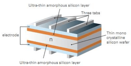
Illustration 9 – HTJ cell section (not to scale), [1]
These cell technologies are all extrapolated to bifacial configurations. This bifacial market (which already has market shares close to 50%), will be predominant in the coming years.
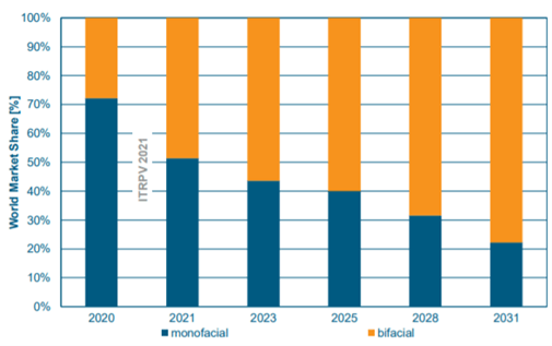
Illustration 10 – Monofacial and bifacial market, [2]
In addition to cell technologies, the market is tending (in its career at a lower LCOE cost), to implement:
- Cell size increase (182mm / 210mm being the sizes that will become standard in the coming years). These larger cell sizes make it possible to reduce spaces between cells, or increase the size of the module, which results in reductions in LCOE.
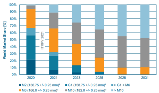
Illustration 12 – Evolution of cell sizes, [2]
- Increase in the number of busbars (Multi Busbar technologies – MBB)
This technology helps to minimize internal electrical losses (by reducing resistive losses), increasing the efficiency of the module.
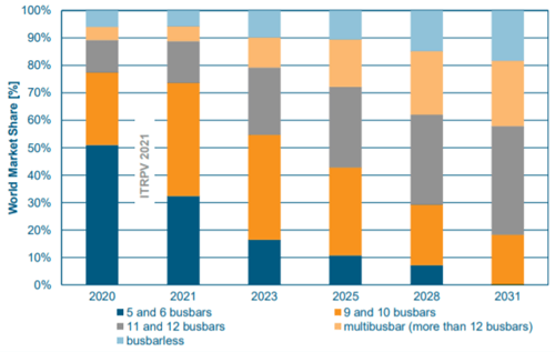
Illustration 13 – Evolution of MBB technology, [2]
- Introduction of split cells (Half-cell)
It allows to reduce currents (and therefore electrical losses), and reduce shadow effects.
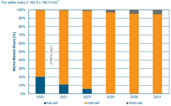
Illustration 14 – Evolution of the cell market by division of the same, [2]
- Reduction of gaps between cells (shingled solar modules, Tiling Ribbon – TR, etc)
By eliminating the gaps between cells, it is possible to increase the power per m2 of surface.In conclusion, we can assure you that the evolution of photovoltaic modules will continue at the current speed (if not higher), and we are in for a few years where we will have to be very aware of the different trends and the bets of each manufacturer for them.References[1] Photovoltaics Technology Development Report, Low Carbon Energy Observatory, EUR 30504 EN
[2] International Terhnology Roadmap for Photovoltaics, 2020 Results, April 2021
